
AlN-on-Si for quantum emitters and sensors (AQUES) – Engineering specific defect formations
The AQUES (AlN-on-Si for Quantum Emitters and Sensors) project commenced at the start of 2025 as a part of the Technology Programme. The main aim is to engineer specific point defects with single photon emission capabilities on high quality aluminium nitride (AlN) grown on Si (111) substrates utilizing metal organic vapor phase epitaxy (MOVPE) for applications in quantum technologies. The key objectives include optimizing MOVPE growth parameters, investigating defect formations on as grown films and their correlation to the growth parameters, engineering specific defect formations via ion implantation processing and annealing to enhance single-photon emission capabilities, and finally characterizing those utilizing advanced optical characterization techniques. This project is a collaborative effort between Aalto University and the University of Helsinki, combining their respective expertise on the research topic. In this blog post, I will provide a brief overview of the project’s background, key concepts, and implementation strategies.
Before diving, lets understand what single photon emitters essentially are and how to characterize and confirm them. Single photon emitters (SPEs) are quantum light sources that produce individual photon with high precision either on-demand or with high probability and are key for realizing exotic applications in the quantum world. SPEs exhibit antibunching which is essentially a quantum mechanical phenomenon where photons are emitted or detected with more uniform temporal spacing than expected from a classical light source. In other words, a SPE cannot emit a second photon immediately after a first one because it needs time to return to its ground state and be re-excited, leading to a reduced probability of detecting closely spaced photons. This behaviour results in sub-Poissonian statistics, which means the variance of the photon count number is less than the mean, a direct indicator of non-classical light, as classical light sources exhibits Poissonian or super-Poissonian statistics. The extent of this effect is quantified using the autocorrelation function, which is the second-order temporal correlation function g(2)(τ), where a value of g(2)(0) < 0.5 at zero-time delay (τ = 0) confirms single-photon emission (an ideal SPE source has g(2)(0) = 0). These measurements are typically performed using a Hanbury Brown and Twiss (HBT) interferometer setup, which uses a beam splitter to divide the emitted light between two detectors to measure the time differences between photon arrival events and build a histogram of these delays.
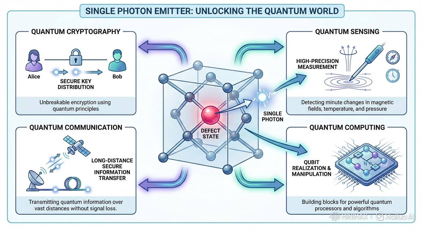
Considering the critical importance of SPEs in quantum applications, a key challenge lies in developing scalable and reliable manufacturing processes to integrate them into current systems and technologies effectively. Before that, lets first briefly go through the different types of SPEs which are available in various forms. SPEs based on quantum dots and trapped ions often necessitate extremely low temperatures to preserve coherence and enable precise control. These systems rely on cryogenic equipment, which complicates scalability. While these emitters perform exceptionally well in controlled laboratory settings, their complex setups hinder practical deployment. On the other hand, defect centres in ultra wide bandgap (UWBG) and wide bandgap (WBG) materials—such as diamond, hexagonal boron nitride, aluminum nitride (AlN), silicon carbide (SiC), and gallium nitride (GaN)—provide a promising avenue for more practical applications. These defect centres, referred to as deep colour centres, can emit single photons even at room temperature. Although such defect centres are undesirable in electronic and optoelectronic devices as it degrades device performance and efficiency, they are highly valued in quantum applications because they offer localized, controllable, and optically addressable spin states for qubits and emit single photons, which are crucial for quantum communication and cryptography. Fig. 1 illustrates the SPE concept based on defect states and their potential applications in the quantum world. The ability to operate at room temperature with scalable manufacturing possibilities positions defect centres in UWBG materials, as strong candidates for developing practical and robust single-photon sources for exotic applications in quantum technologies and systems.
In AQUES project, our focus is on engineering specific point defects in AlN due to its remarkable physical properties. AlN boasts an ultra-wide band gap of 6.2 eV, high electrical resistivity exceeding (>1013 Ω.cm), superior thermal conductivity reaching up to 318 W/m·K, and compatibility with CMOS manufacturing processes. These attributes make AlN highly suitable for a variety of applications, including photonics, microelectromechanical systems (MEMS), and power devices. Moreover, AlN could be deposited by physical vapour deposition (PVD) and epitaxial processes like MOVPE and molecular beam epitaxy (MBE) on different substrates. Epitaxial processes at high temperatures (≈ 1000 °C) gives significant freedom in tailoring the material properties with high crystal quality and enhanced control over contamination, surface roughness, and defects.
Literature shows that SPEs have been found in epitaxially grown AlN films on sapphire and Si substrates with emission in the visible to near infrared at room temperature. However, these emitters are randomly distributed presenting challenges in terms of predictability and manufacturing [1]. The randomness of the distribution of these emitters can complicate efforts to design devices with precise and reliable quantum properties. To improve their performance and uniformity, it is crucial to engineer specific defect formations. This can be achieved through ion implantation followed by thermal annealing to activate the defects. Recent research has demonstrated the creation of SPEs using ion implantation of elements such as helium (He), zirconium (Zr), krypton (Kr), and aluminum (Al) in AlN thin films [2-4]. For Zr, the theoretical predictions for the formation of stable complexes with nitrogen vacancies ZrAlVN [5] were confirmed experimentally in [4], however similar defects emitting in the same spectral range were also observed in as-grown AlN and AlN films implanted with Kr. This also highlighted the problem of depending solely on fluorescence for SPE confirmation with predictable properties. Therefore, achieving optimal results requires meticulous theoretical planning to predict and control defect behaviour, complemented by comprehensive experimental characterization to verify the quality and consistency of the SPE sources. Such methodologies enable targeted manipulation of material properties to produce emitters with desired characteristics.
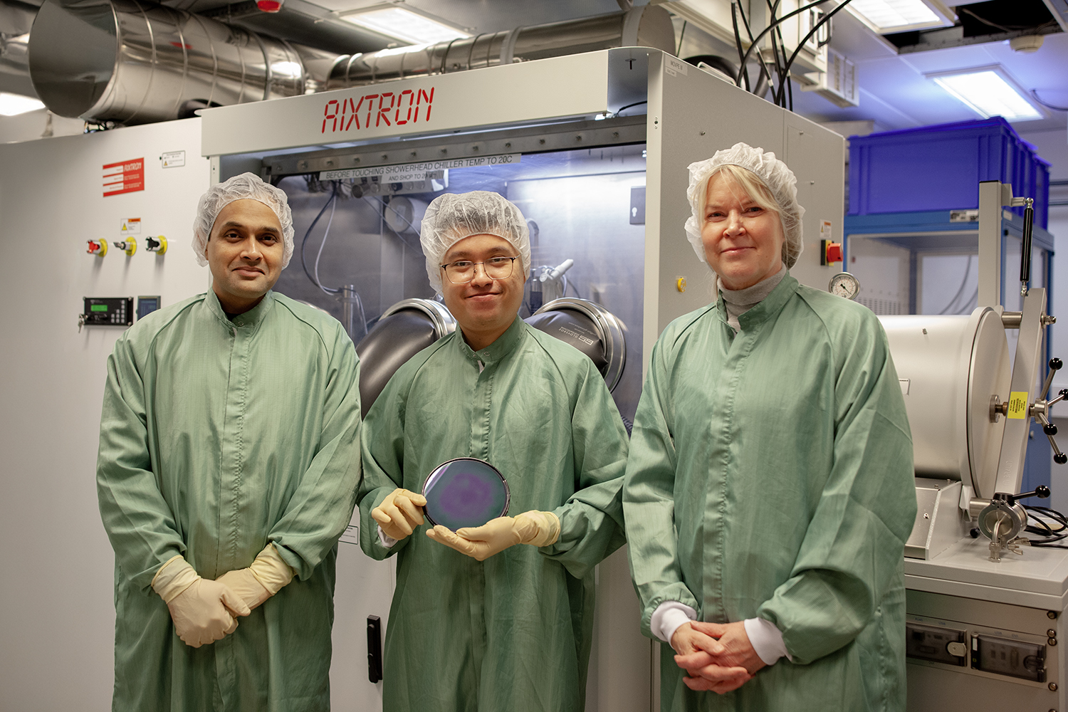
In AQUES, the implementation strategy for engineering point defects as SPEs require a thorough understanding of their formation and their relation to the MOVPE growth process parameters. Using Aalto University’s Aixtron MOVPE reactor, high-purity single-crystal AlN will be grown on Si (111) substrates. The reactor features advanced in-situ monitoring systems and a specialized showerhead gas injector to minimize unwanted precursor pre-reactions, complemented by a high-temperature heater capable of reaching 1500 °C crucial for producing high-quality Al-containing III-N alloys. The MOVPE process parameters will be optimized to produce AlN layers with minimal defects and impurities across 150 mm Si wafers. The as grown AlN films will be characterized for its crystal quality, strain, morphology using advanced techniques, such as HRXRD, AFM, SEM, and TEM. The defects and trap states at the AlN-Si interface will also be characterized electrically.
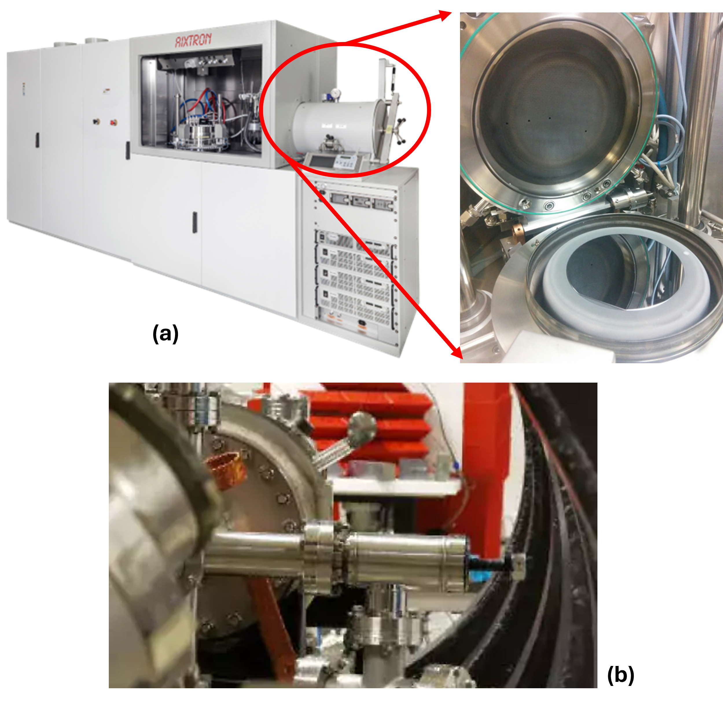
Prior to ion implantation experiments, an in-depth characterization of impurity levels is essential to assess the film quality, identify inherent impurities, and determine their charge states. The point defect states (vacancies, antisites), impact of impurities (e.g., carbon) and inherent impurities in silicon wafers (e.g., O, N) and their complexes on bulk AlN and the AlN-Si interface will be investigated using advanced characterization techniques available at the Accelerator Laboratory. The laboratory’s state-of-the-art facilities include a recently upgraded 5 MV tandem accelerator, a 500 kV accelerator/ion implanter, and two slow positron beams. Associated analysis methods include particle-induced X-ray emission (PIXE), elastic recoil detection analysis (ERDA), Rutherford backscattering spectroscopy (RBS), accelerator mass spectrometry (AMS), and positron annihilation-based lifetime and Doppler broadening spectroscopies. Experiments can be performed in a wide temperature range from 1500 K down to cryogenic temperatures in the mK regime. Fig. 2 shows the key tools – Aalto’s MOVPE reactor and Accelerator Laboratory’s positron annihilation spectroscopy (PAS) which will be extensively utilized in the project.
After MOVPE process optimization, initial microstructural and electrical characterization, samples with various AlN thicknesses ranging from hundreds of nanometers to a few microns, will be prepared for further investigations. Ion implantation at the Accelerator Laboratory of the University of Helsinki will introduce various dopants into these optimized AlN layers with the aim of engineering specific defect formations that serve as single photon emission sources. A wide array of ion species, implantation energies, and fluences will be explored to identify optimal processing conditions. Subsequent optical characterization, including continuous wave and pulsed autocorrelation measurements, will assess the single photon emission capabilities of these engineered defects.
There will be active collaboration between Electronics integration and reliability group (EILB) of Aalto University and Helsinki Accelerator laboratory of University of Helsinki. The project will extensively utilize facilities in Otaniemi micro- and nano-technology research infrastructure (OtaNano): Micronova and Nanomicroscopy center for the growth of AlN, microstructural and electrical characterization, and facilities in Helsinki Accelerator Laboratory for in depth material characterization, ion implantation and optical characterization.
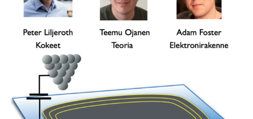
The research group comprise of the following researchers: Dr. Nikhilendu Tiwary (Project leader, AU), Mr. Josef Stevanus (AU), Prof. Mervi Paulasto-Kröckel (AU), Ms. Wen Xi (UoH), Dr. Igor Prozheev (UoH), Dr. Ilja Makkonen (UoH), Prof. Filip Tuomisto (UoH), and Dr. Matti Kalliokoski (UoH).
If successful, the research efforts in AQUES will pave the way for more practical and remarkable applications in the quantum world such as quantum sensing, quantum cryptography, quantum communication and quantum computing.
Nikhilendu Tiwary
Staff Scientist at Aalto University
Project Leader (AQUES ) at Helsinki Institute of Physics
References:
[1] J. K. Cannon et al., “Room temperature quantum emitters in aluminum nitride epilayers on silicon”, Applied Physics Letters, vol. 124, 244001, 2024.
[DOI: https://doi.org/10.1063/5.0207744]
[2] T-J. Lu et al., “Bright High-Purity Quantum Emitters in Aluminum Nitride Integrated Photonics”, ACS Photonics, vol. 7, 2650-2657, 2020.
[DOI: https://doi.org/10.1021/acsphotonics.0c01259]
[3] H.B. Yagci et al., “Tracking the creation of single photon emitters in AlN by implantation and annealing”, Optical Materials, vol. 156, 115967, 2024.
[DOI: https://doi.org/10.1016/j.optmat.2024.115967]
[4] A. Senichev et al., “Quantum emitters in aluminum nitride induced by heavy ion irradiation”, APL Quantum, vol. 1, 036103, 2024.
[DOI: https://doi.org/10.1063/5.0199647]
[5] J. B. Varley, A. Janotti, C. G. Van de Walle, “Defects in AlN as candidates for solid-state qubits”, Physical Review B, vol. 93, 161201(R), 2016.
[DOI: http://dx.doi.org/10.1103/PhysRevB.93.161201]